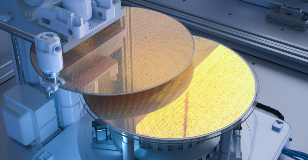
A thermal oxide silicon wafer is a silicon wafer that has been coated with a layer of silicon dioxide, also known as silica or glass, using a process called thermal oxidation. This process involves heating the silicon wafer in an oxygen-rich environment at a high temperature, typically between 800 and 1200 degrees Celsius, for a period of time. As the wafer is heated, the oxygen reacts with the silicon to form silicon dioxide on the surface of the wafer.
Thermal Oxide Silicon Wafer Properties
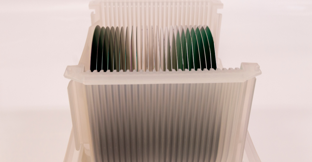
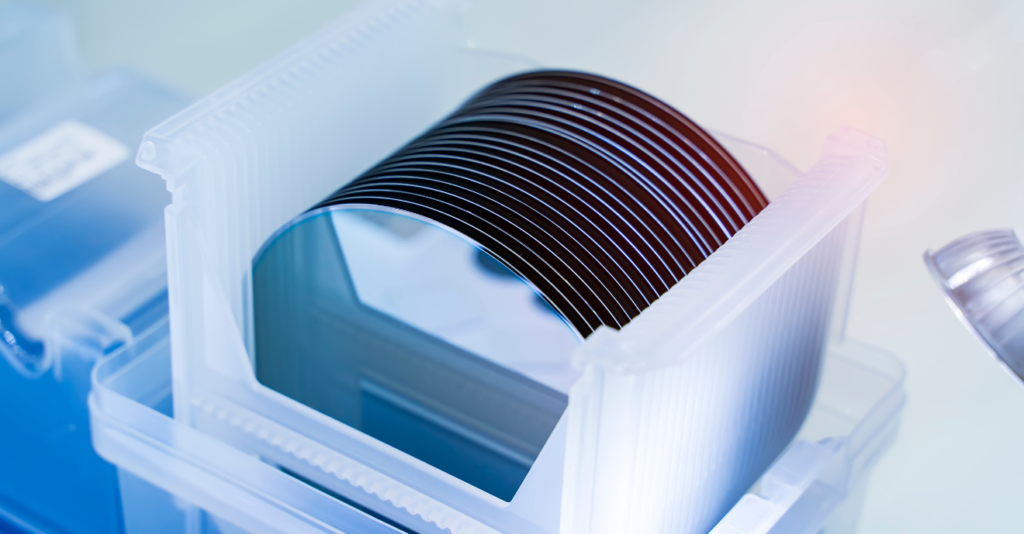
Thermal Oxide Silicon wafers are semiconductor disks made from high-quality silicon material that is oxidized on the surface through a thermal process. These disks are used for many different industrial applications. Below are the properties of Thermal Oxide Silicon wafers that are produced as standard.
- P-type and N-type options are available.
- Dimensions: 2 inches, 3 inches, 4 inches, 5 inches, 6 inches, 8 inches, 12 inches
- Thickness: Thicknesses between 300nm – 10μm are available.
- Oxide Thickness: Oxide thicknesses between 100nm – 500nm are available.
- Surface Roughness: Roughnesses between Ra < 0.5nm – Ra < 5nm are available.
- Oxide Grade: Standard, Thermal Oxide Grade 1, Thermal Oxide Grade 2
- Orientation: {100}, {111}, {110}
- Surface Treatment: Single Side Polished (SSP), Double Side Polished (DSP), Double Side Mirror Polished (DSMP)
- Measurement Method: TTV (Total Thickness Variation) and BOW (Bow/Warp)
- Packaging: Wafer Shipping Box, Wafer Shipping Carrier
The above properties are typical properties for Thermal Oxide Silicon wafers produced as standard. The available properties may vary depending on the details and specifications of the order.
Thermal oxide silicon wafers are used in a wide range of electronic devices, including integrated circuits, microelectromechanical systems (MEMS), and solar cells. They are also used as a substrate for thin-film deposition processes, such as sputtering or chemical vapor deposition, in the manufacture of advanced electronic devices.
The properties of the thermal oxide layer can be modified by adjusting the thickness of the layer, the temperature and duration of the thermal oxidation process, and the concentration of oxygen in the environment. This allows manufacturers to tailor the properties of the thermal oxide layer to meet the specific requirements of their applications.