Silicon wafer are an essential component in the production of a wide range of electronic devices, including computers, smartphones, and other consumer electronics, as well as industrial and medical devices. They are also used in the production of photovoltaic cells for solar panels.
The products we offer as standard are:
| Wafer Size | Diameter (mm) | Thickness (mm) | Surface Type | Resistivity (Ohm-cm) | Dopant Type |
| 2 inch | 50.8 | 0.279 – 0.381 | P or N | 0.001 – 100 | Boron or Phosphorus |
| 3 inch | 76.2 | 0.381 – 0.508 | P or N | 0.001 – 100 | Boron or Phosphorus |
| 4 inch | 100 | 0.525 – 0.785 | P or N | 0.001 – 100 | Boron or Phosphorus |
| 5 inch | 125 | 0.625 – 1.025 | P or N | 0.001 – 100 | Boron or Phosphorus |
| 6 inch | 150 | 0.625 – 1.525 | P or N | 0.001 – 100 | Boron or Phosphorus |
| 8 inch | 200 | 0.725 – 2.525 | P or N | 0.001 – 100 | Boron or Phosphorus |
| 12 inch | 300 | 0.775 – 2.525 | P or N | 0.001 – 100 | Boron or Phosphorus |
Silicon Wafer Using Area
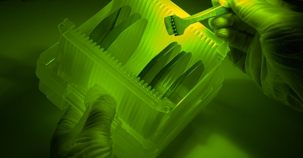
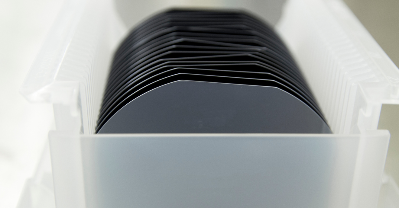
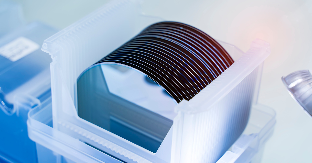
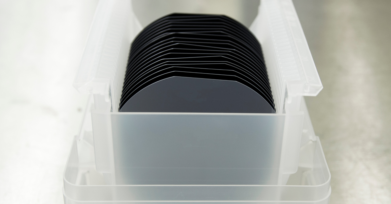
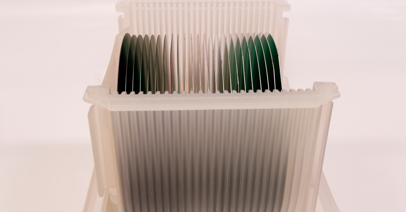
A silicon wafer is a thin slice of semiconductor material, typically silicon, that is used as a substrate in the fabrication of electronic devices such as microprocessors, sensors, and solar cells. Silicon wafers are typically round and flat, with a diameter ranging from a few millimeters to several inches.
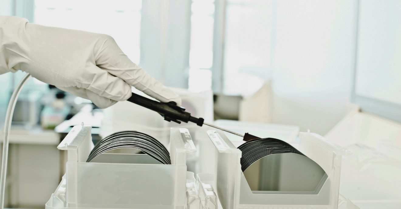
Silicon wafers are produced through a process called wafer fabrication, which involves several steps including growing a silicon crystal, slicing it into thin wafers, and polishing the surface to achieve a high level of surface finish. Silicon wafers are then used as a substrate upon which various layers of materials are deposited and patterned to create the desired electronic devices.
- High purity: Silicon wafers are made from highly purified silicon, with impurity levels typically in the parts per billion (ppb) range. This high level of purity is important for the performance and reliability of electronic devices.
- Good electrical properties: Silicon has excellent electrical properties, including a high electron mobility, which makes it an ideal material for use in electronic devices.
- High thermal conductivity: Silicon has a high thermal conductivity, which allows it to dissipate heat efficiently, making it suitable for use in high-power devices.
- High melting point: Silicon has a high melting point, making it resistant to thermal degradation.
- High mechanical strength: Silicon wafers have good mechanical strength, making them suitable for use in high-stress environments.
- High chemical stability: Silicon is resistant to most chemicals, making it suitable for use in a wide range of applications.


