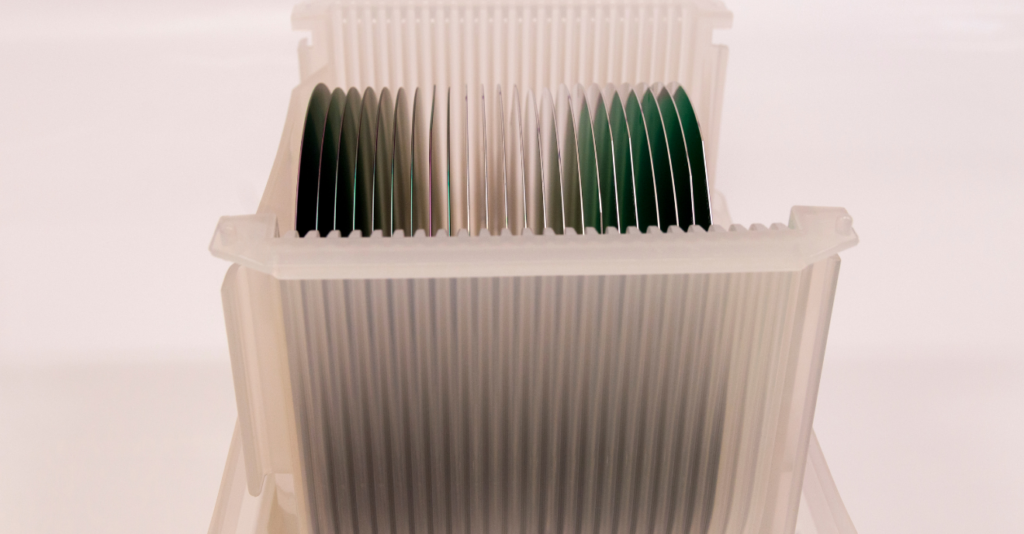
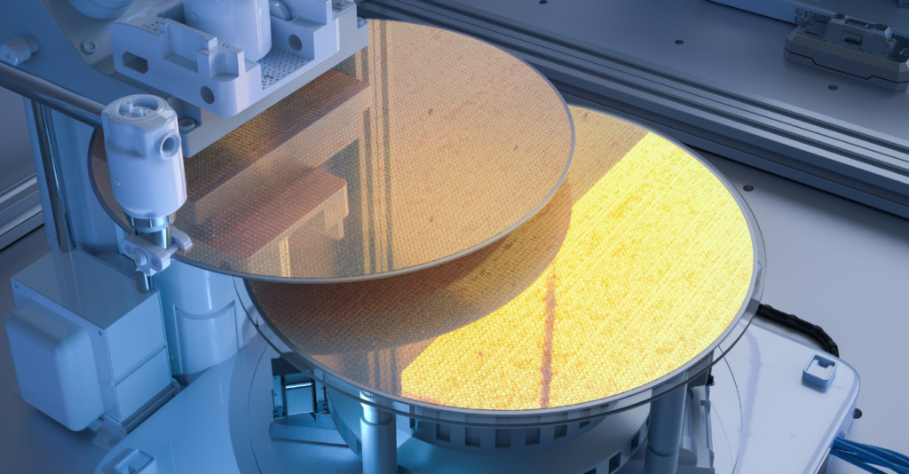
Silicon carbide (SiC) wafer is a semiconductor material that is used in the production of electronic and optoelectronic devices. SiC wafers are thin, circular discs of SiC that are used as a substrate material in the manufacturing of these devices.
SiC is known for its high thermal conductivity, high electron mobility, and high breakdown voltage, which make it useful in a variety of high-power and high-temperature applications. It is used in the production of transistors, diodes, and other electronic devices that are capable of operating at high power levels and high temperatures.
SiC wafers are used in a variety of applications, including power electronics, energy storage, renewable energy, and telecommunications. They are particularly useful in applications that require the ability to operate at high power levels and high temperatures.
There are several key specifications to consider when working with SiC wafers:
- Diameter: SiC wafers are typically available in a range of diameters, including 2 inches, 3 inches, 4 inches, and 6 inches. The diameter of the wafer can affect the cost and performance of the devices that are manufactured on it.
- Thickness: SiC wafers are available in a range of thicknesses, typically ranging from 100 micrometers to 750 micrometers. The thickness of the wafer can affect the strength and flexibility of the devices that are produced on it.
- Dopant concentration: SiC wafers can be doped with impurities such as aluminum or nitrogen to modify their electrical properties. The concentration of dopants in the wafer can affect the performance of the devices that are manufactured on it.
- Surface roughness: The surface roughness of SiC wafers can affect the quality of the devices that are produced on them. SiC wafers with a smooth surface may be preferred for certain applications, such as the production of high-quality integrated circuits.
- Crystalline quality: The crystalline quality of SiC wafers can affect the performance of the devices that are produced on them. SiC wafers with high crystalline quality may be preferred for certain applications, such as the production of high-performance transistors.
| Parameter | Description |
| Wafer Diameter | The diameter of the wafer, measured in inches. Typical range is 2-6 inches. |
| Wafer Thickness | The thickness of the wafer, measured in microns. Typical range is 150-2000 microns. |
| Wafer Polarity | The polarity of the wafer, either Semi-insulating or N-type. |
| Wafer Orientation | The crystal orientation of the wafer, measured by its Miller indices. Typical values are (0001) or (000-1) off-axis. |
| Wafer Surface Finish | The surface finish of the wafer, either single or double-sided polished. |
| Resistivity | The resistivity of the wafer, measured in Ohm-cm. Typical range is 0.005-10,000 Ohm-cm. |
| Carrier Concentration | The carrier concentration of the wafer, measured in cm^-3. Typical range is 1e16-1e21 cm^-3. |
| Micropipe Density | The density of micropipes in the wafer, measured in cm^-2. Micropipes are defects in the crystal structure that can cause electrical failures in devices. Typical range is less than 5 cm^-2. |
| Dislocation Density | The density of dislocations in the wafer, measured in cm^-2. Dislocations are defects in the crystal structure that can affect device performance. Typical range is less than 1e6 cm^-2. |
| Threading Dislocation Density | The density of threading dislocations, a specific type of dislocation that can originate from the substrate and extend into the epitaxial layer. This parameter is particularly important for power devices, and typical range is less than 1e4 cm^-2. |