
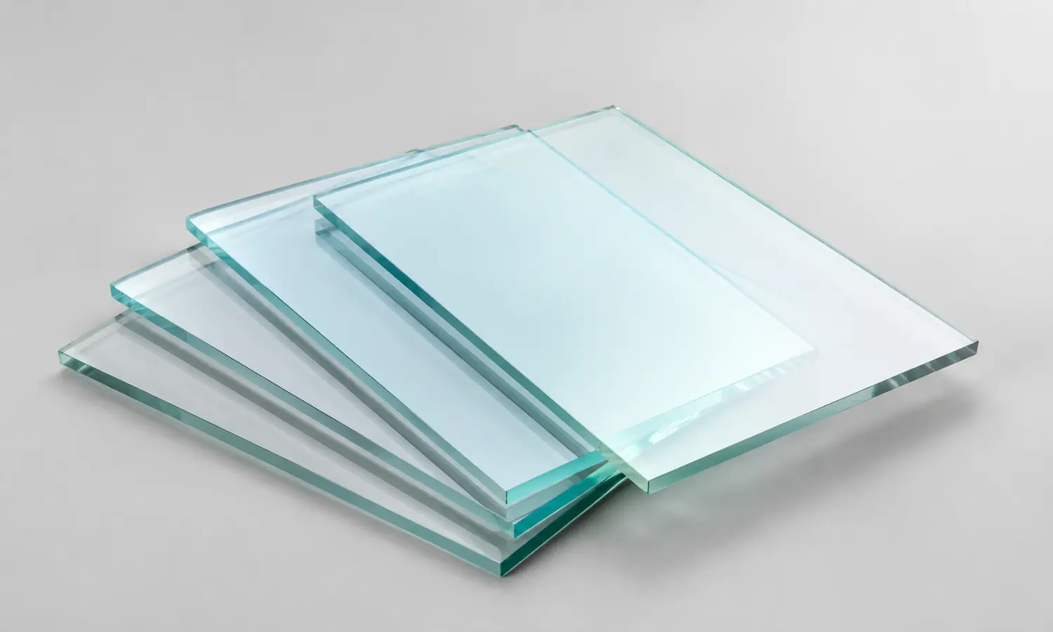
ITORepresentative visual
ITO Coated Glass Substrate
Transparent conductive ITO glass with selectable resistance.
- Sheet resistance
- 5–100 Ω/sq typical
- Thickness
- 0.4–3 mm
Custom vacuum chamber design and manufacturing; technical supply of vacuum components, wafers, deposition targets and conductive glass.
Custom compositions and non-listed products are welcome. No account registration needed.
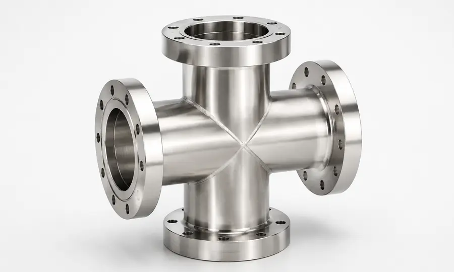
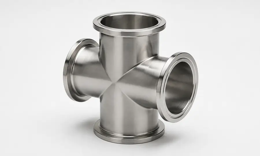
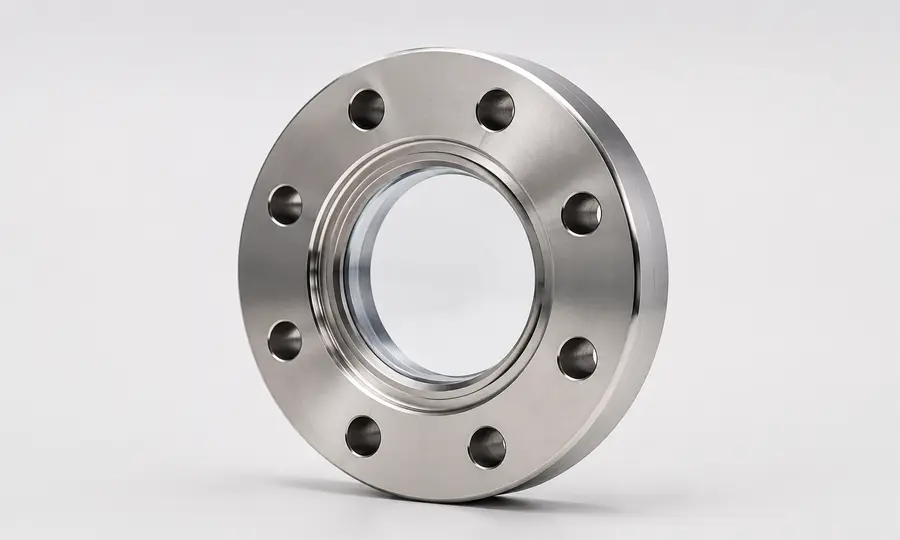
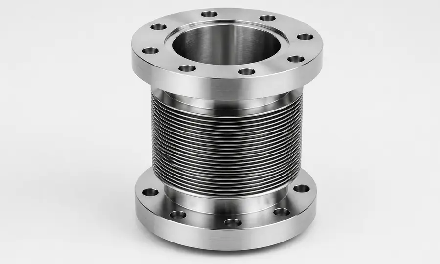
Custom process chambers, KF–CF–ISO components, viewports, bellows and system integration.
Enter vacuum division →02 · SEMICONDUCTOR MATERIALSWafers, sputtering targets, evaporation materials, conductive glass and high-purity research materials.
Enter semiconductor division →Search if you know the product. If the specification is still taking shape, share what you know and our team will clarify the missing details.
Explore KF, CF, ISO, viewports and bellows.
Start here →02Search by formula, material name or product code.
Start here →03Describe your process and system requirements.
Start here →04Describe a custom composition, geometry or application.
Start here →No. Share the material, dimensions and application you know. Mention any uncertainties in your notes; the technical team clarifies the requirements before quotation.
Yes. Combine catalogue products and custom requirements in the same RFQ.
You receive a reference number. Our team reviews technical suitability and clarifies missing details by email. Price and lead time are provided in the formal quotation.
Choose a product family, specify the technical requirements and combine products from different groups in one quotation list.
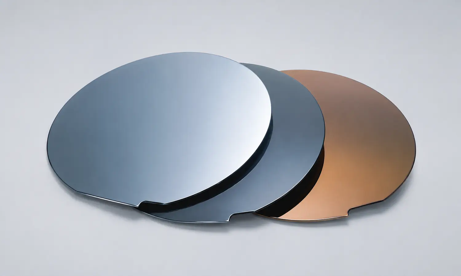
Si, SiO₂, GaAs, GaSb, GaN, SiC and sapphire substrates.
View family ↗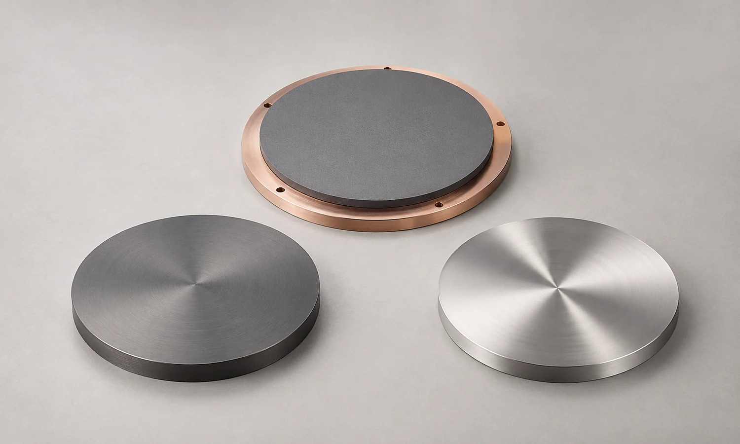
Pure metals, alloys, oxides and ceramic targets with optional backing plate.
View family ↗ITO and FTO coated glass with selectable resistance and cut sizes.
View family ↗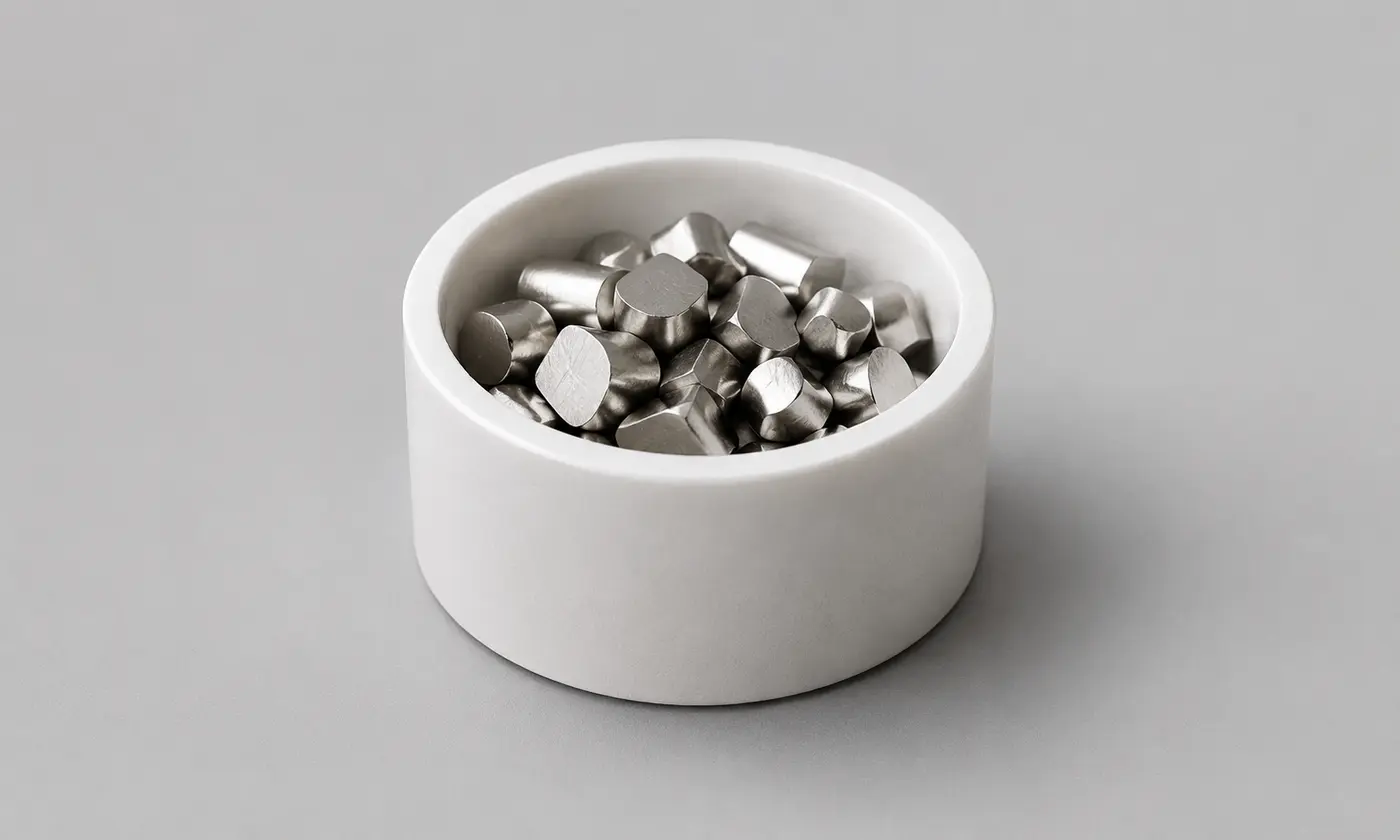
High-purity elemental source materials supplied with analysis documentation.
View family ↗Transparent conductive ITO glass with selectable resistance.
Prime, test and research-grade silicon substrates.
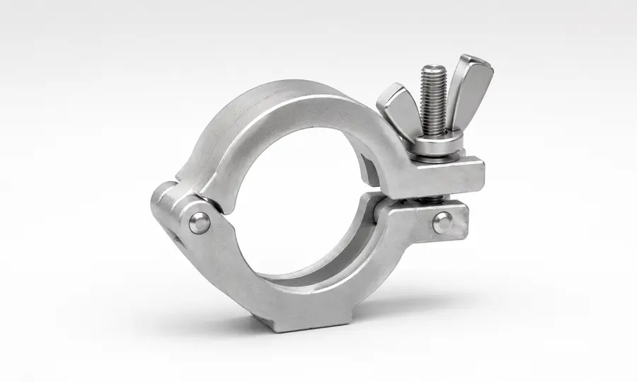
Aluminium quick clamp for joining two KF flanges.
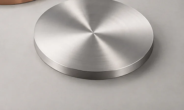
High-purity Titanium (Ti) sputtering target for PVD and thin-film deposition.
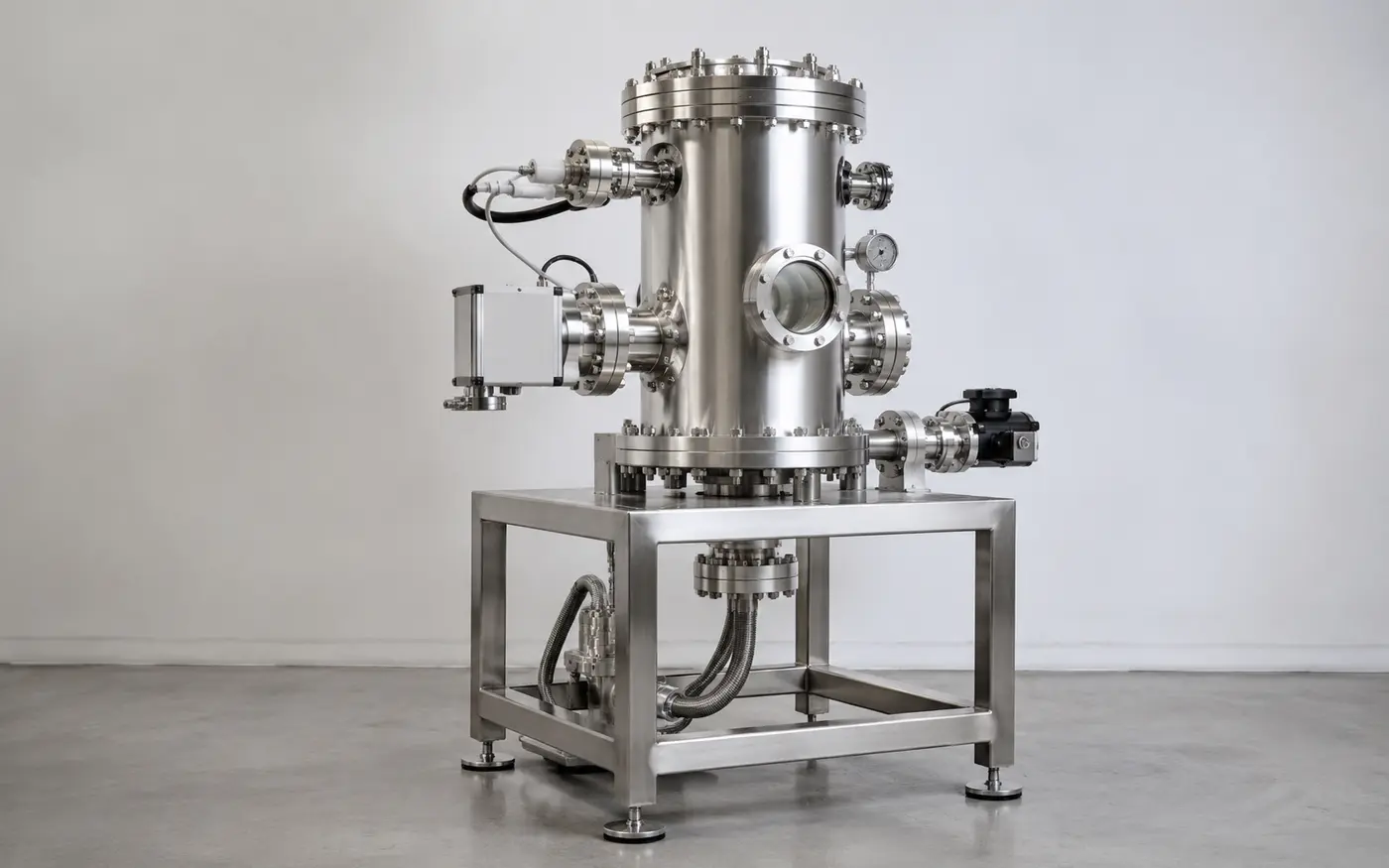
Adesis designs and manufactures stainless-steel vacuum chambers for thin-film, plasma, optical-test and special R&D processes. Chamber volume, access doors, port layout, feedthroughs, viewports, pumping lines and instrument interfaces are evaluated together at the start of the project.
KF, CF and ISO connection hardware, viewports and flexible elements supplied individually or integrated into engineered assemblies.
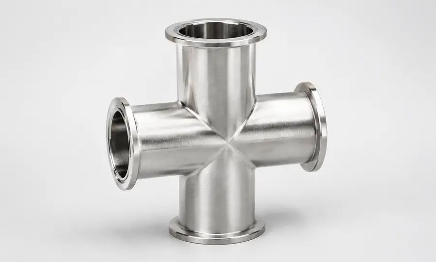
Material, geometry, finish and application.
Technical team reviews the requested specification.
Analysis certificate and shipment documentation.
DAP or EXW shipment from Türkiye.
Customer names, project identities and production photographs remain confidential. These briefs describe representative engineering scopes reviewed by Adesis.
Coordinated source ports, substrate motion, viewport, gas inlet and pumping interfaces.
Clear aperture, window material, beam path, thermal load and instrumentation interfaces.
Serviceable port layout, sensor feedthroughs and mechanical provision for future integration.