Indium antimonide (InAs) is a semiconductor material that belongs to the group III-V family of compounds, which are composed of elements from the periodic table’s third and fifth columns. InAs has a narrow bandgap and high electron mobility, making it useful in a variety of electronic and optoelectronic devices. It is often used to make high-speed transistors, lasers, and detectors for infrared and terahertz radiation.
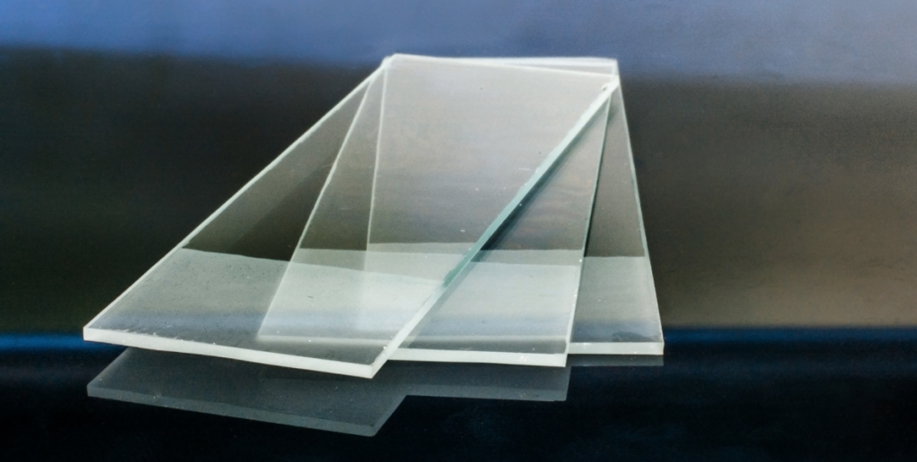
A wafer is a thin slice of a semiconductor material, such as InAs, that is used as a substrate for the growth or fabrication of electronic devices. Wafers are typically round or rectangular in shape and are made by slicing a block of semiconductor material, known as a boule, into thin layers using a process called wafering. The wafer is then polished to a smooth finish and undergoes various processing steps, such as doping and deposition, to create the desired electronic devices.
The specifications of an InAs wafer can vary depending on the specific application and the manufacturer. Some of the key specifications to consider when selecting an InAs wafer include:
- Diameter: The size of the wafer, usually measured in millimeters.
- Thickness: The thickness of the wafer, usually measured in micrometers.
- Doping type and concentration: The type and concentration of impurities (dopants) added to the wafer to alter its electrical properties.
- Crystal orientation: The orientation of the crystal lattice in the wafer, which can affect its electrical and optical properties.
- Surface finish: The smoothness and quality of the wafer’s surface, which can affect the performance of devices fabricated on the wafer.
- Purity: The level of impurities present in the wafer, which can affect the performance and reliability of devices fabricated on the wafer.
- Resistance: The electrical resistance of the wafer, which can affect its performance in certain applications.
- Mobility: The electron mobility of the wafer, which determines how quickly electrons can move through the material and can affect the performance of high-speed devices.
- Bandgap: The energy gap between the valence and conduction bands in the wafer, which determines its ability to conduct electricity and can affect its use in optoelectronic devices.