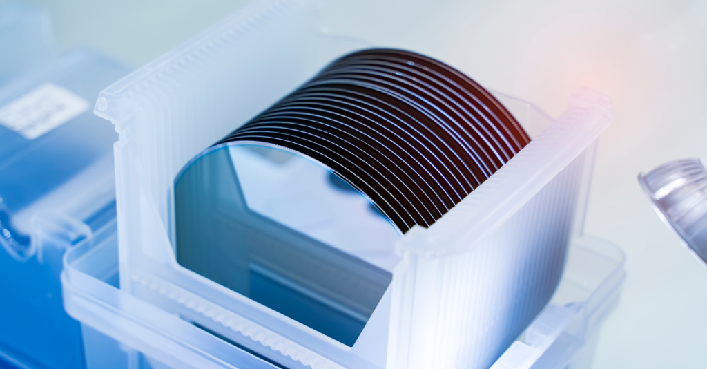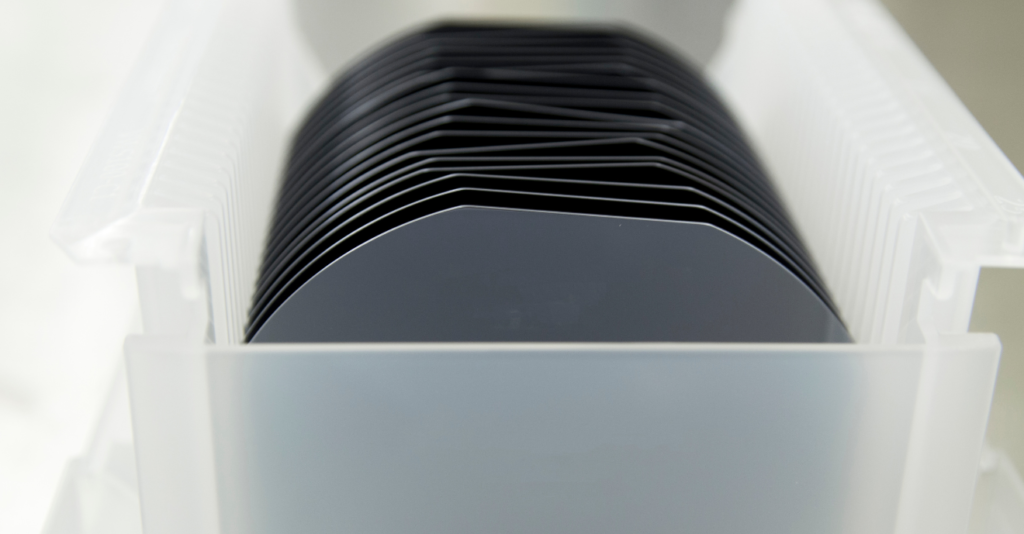
Gallium nitride (GaN) wafer is a semiconductor material that has a wide bandgap and a high breakdown voltage, making it suitable for use in high-power and high-frequency electronic devices. GaN wafers are thin, circular discs of GaN material that are used as the substrate in the production of electronic devices such as high-power transistors, LED lights, and microwave electronics.
GaN has a number of properties that make it attractive for use in these applications, including high thermal stability, good electrical conductivity, and excellent radiation resistance. It is also able to operate at high temperatures and high power levels, making it suitable for use in demanding environments.
GaN wafers are typically grown using a process called metalorganic chemical vapor deposition (MOCVD), in which GaN material is deposited on a substrate using a chemical reaction. The GaN wafer is then polished to a smooth finish and cut into smaller wafers for use in the production of electronic devices
| Property | Values |
|---|---|
| Dimensions | |
| Diameter | 2 inches (50.8 mm), 4 inches (101.6 mm), 6 inches (152.4 mm) |
| Thickness | 350 µm, 500 µm, 675 µm |
| Surface Orientation | |
| C-Plane | 0001 |
| M-Plane | 10-10 |
| A-Plane | 11-20 |
| Electrical Properties | |
| Carrier Density | 5×10¹⁸ /cm³ – 2×10¹⁹ /cm³ |
| Resistivity | 0.1 – 10 Ω·cm |
| Compatibility | |
| Si | Yes |
| GaN | Yes |
| SiC | Yes |
GAN-FS WAFER is a type of gallium nitride (GAN) on silicon carbide (SiC) substrate that is used as a material in the manufacturing of high-power electronics and optoelectronic devices. It is primarily used in the production of power electronic devices, such as high-voltage power transistors, high-frequency power amplifiers, and high-power microwave devices, as well as in the manufacturing of LED lighting systems.
The use of GAN-FS WAFER allows for the production of high-performance electronic devices that are capable of operating at high temperatures, high voltage, and high power levels. This makes it particularly useful in a variety of applications, including power conversion, energy storage, renewable energy, and telecommunications. It is also used in military and aerospace applications, where the ability to withstand extreme conditions is important.
GAN TEMPLATES WAFER is a type of gallium nitride (GAN) substrate that is used as a template in the production of high-performance electronic devices. The term “template” refers to the fact that the GAN TEMPLATES WAFER serves as a base material onto which other layers of materials are deposited, using a process called epitaxial growth.
GAN TEMPLATES WAFER is typically used in the production of high-power electronic devices, such as high-voltage power transistors, high-frequency power amplifiers, and high-power microwave devices. It is also used in the manufacturing of LED lighting systems. The use of GAN TEMPLATES WAFER allows for the production of high-performance electronic devices that are capable of operating at high temperatures, high voltage, and high power levels.
GAN TEMPLATES WAFER is used in a variety of applications, including power conversion, energy storage, renewable energy, and telecommunications. It is also used in military and aerospace applications, where the ability to withstand extreme conditions is important.
GAN HEMT EPITAXIAL WAFER is a type of gallium nitride (GAN) substrate that is used as a base material in the production of high-electron-mobility transistors (HEMTs). HEMTs are a type of high-frequency transistor that are used in a variety of electronic devices, including radio-frequency (RF) amplifiers, mixers, and oscillators.
GAN HEMT EPITAXIAL WAFER is used as a base material because it provides a high-quality, single-crystalline surface onto which layers of other materials can be deposited using a process called epitaxial growth. This allows for the production of high-performance HEMTs that are capable of operating at high frequencies and high power levels.
GAN HEMT EPITAXIAL WAFER is used in a variety of applications, including telecommunications, military and aerospace systems, and consumer electronics. It is particularly useful in RF and microwave applications, where the ability to operate at high frequencies is important.