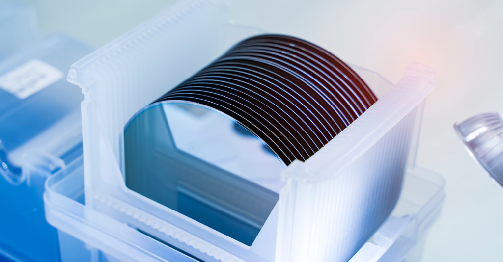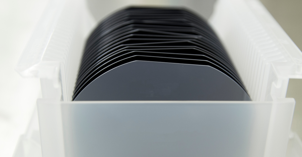
Gallium arsenide (GaAs) wafer is a semiconductor material that is used in the production of electronic and optoelectronic devices. GaAs wafers are thin, circular discs of GaAs that are used as a substrate material in the manufacturing of these devices.
GaAs is known for its high electron mobility, which makes it useful in the production of high-speed electronic devices such as transistors, integrated circuits, and solar cells. It is also used in the production of optoelectronic devices, such as light-emitting diodes (LEDs) and lasers, due to its ability to efficiently convert electricity into light.
GaAs wafers are used in a variety of applications, including telecommunications, military and aerospace systems, and consumer electronics. They are particularly useful in high-speed electronic and optoelectronic applications, where the ability to operate at high frequencies and high power levels is important.
Gallium Arsenide (GaAs) wafers are widely used in the production of electronic and optoelectronic devices. Here are the standard specifications for Our GaAs wafers:
Wafer Diameter
The standard diameter for GaAs wafers is 2 inches, 3 inches, 4 inches, or 6 inches.
Wafer Thickness
The standard thickness for GaAs wafers is 350 microns. Other thicknesses such as 625 microns and 725 microns are also available.
Orientation
The standard orientation for GaAs wafers is (100), (111)A or (111)B. Customized orientations can also be provided upon request.
Dopant Type
The standard dopant type for GaAs wafers is Undoped, S-doped, or Si-doped. Other dopant types can also be provided upon request.
Surface Finish
The standard surface finish for GaAs wafers is Single-side polished (SSP) or Double-side polished (DSP).
TTV
The standard Total Thickness Variation (TTV) for GaAs wafers is <10 microns.
Bow and Warp
The standard Bow and Warp for GaAs wafers is <40 microns.
Resistivity
The standard resistivity range for GaAs wafers is 0.001 – 1000 Ohm-cm.
Carrier Concentration
The standard carrier concentration range for GaAs wafers is 1E14 – 1E19 cm^-3.
These are the standard specifications for GaAs wafers. Specific requirements can be customized based on customer needs.
| Property | Standard Value |
|---|---|
| Wafer Diameter | 2 inches, 3 inches, 4 inches, or 6 inches |
| Wafer Thickness | 350 microns (other thicknesses available) |
| Orientation | (100), (111)A or (111)B (customized orientations available) |
| Dopant Type | Undoped, S-doped, or Si-doped (customized types available) |
| Surface Finish | Single-side polished (SSP) or Double-side polished (DSP) |
| TTV | <10 microns |
| Bow and Warp | <40 microns |
| Resistivity | 0.001 – 1000 Ohm-cm |
| Carrier Concentration | 1E14 – 1E19 cm^-3 |
Above is the table of standard specifications for GaAs wafers. Specific requirements can be customized based on customer needs.