
One technical supply point from wafers to thin-film source materials.
Semiconductor wafers, PVD source materials, conductive substrates and advanced research materials are organized into clear catalogues. Add products from every family to one multi-item RFQ.
 Representative visual
Semiconductor Wafers
Si, SOI, thermal-oxide Si, GaAs, GaN, SiC, InAs, GaSb and sapphire substrates.
Open catalogue →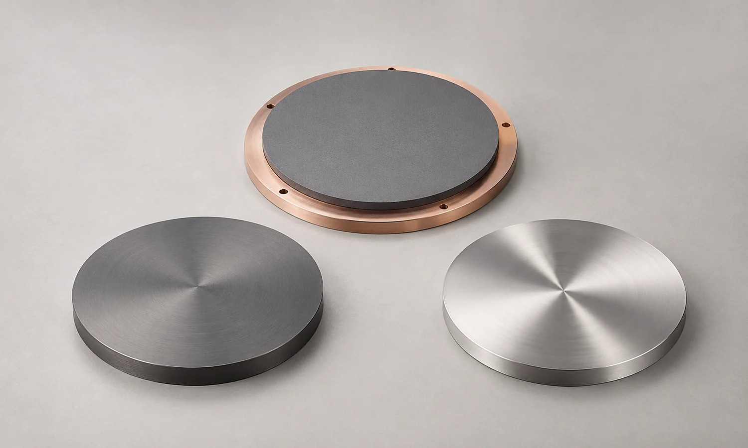 Representative visual
Sputtering Targets
Pure metal, alloy, oxide, nitride, carbide and ceramic targets in standard or custom geometry.
Open catalogue →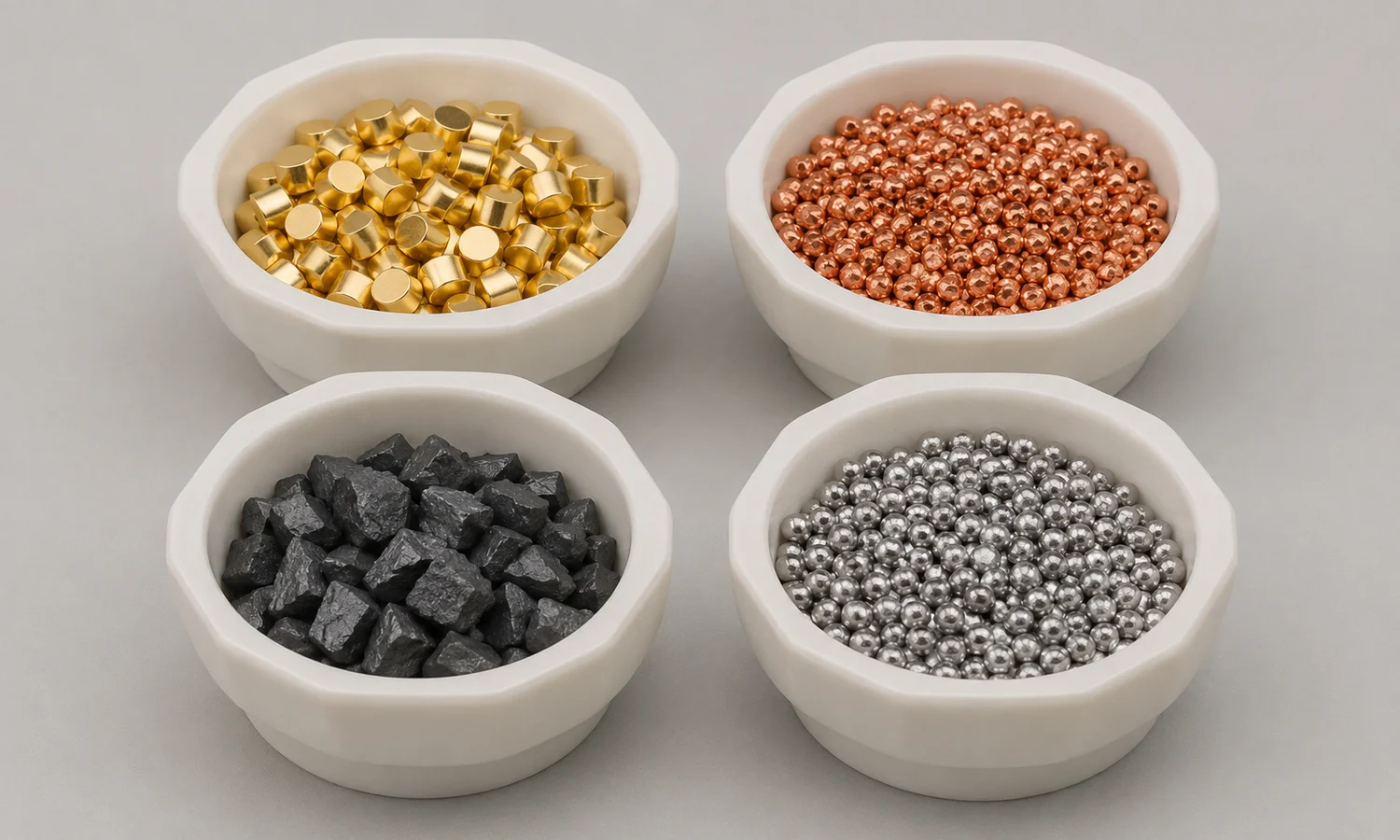 Representative visual
Evaporation Materials
Pellets, granules, shots, pieces and ingots for thermal and e-beam evaporation.
Open catalogue →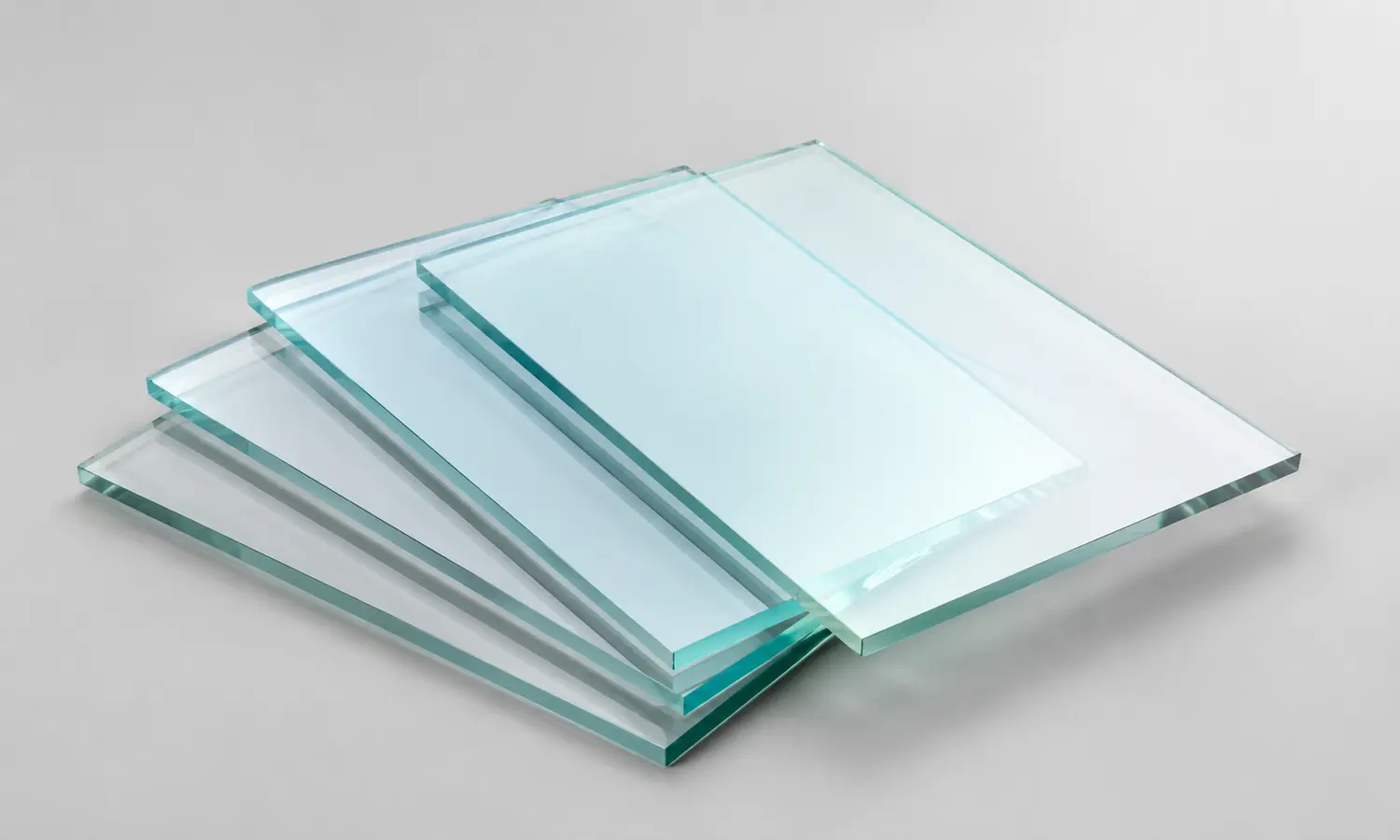 Representative visual
Conductive Coated Glass
ITO and FTO coated glass with selectable sheet resistance and cut dimensions.
Open catalogue →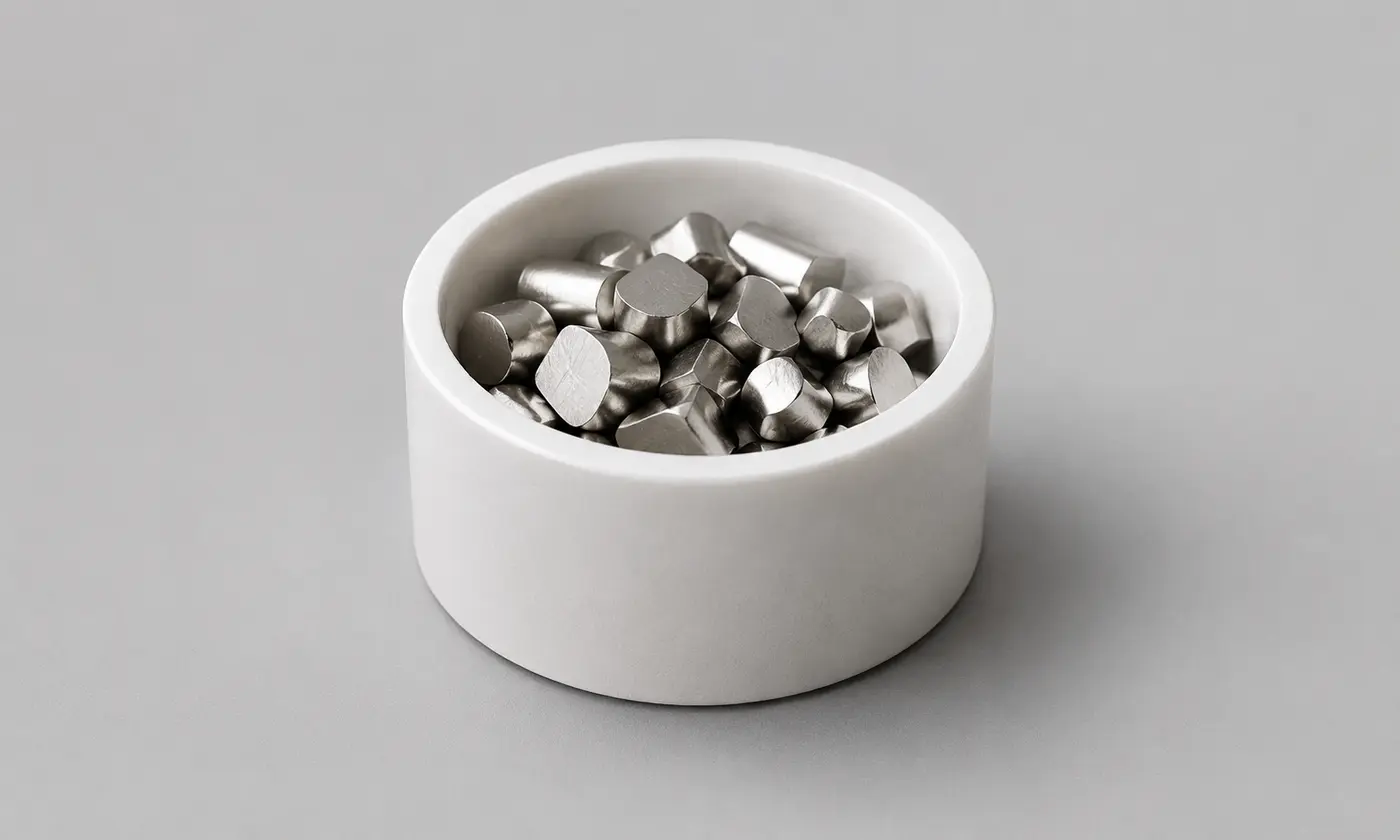 Representative visual
MBE Source Materials
High-purity source materials for III–V and other epitaxy research.
Open catalogue →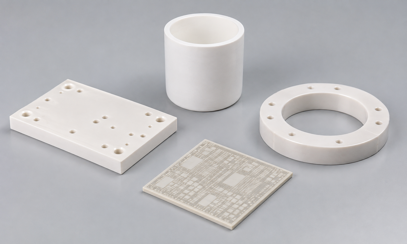 Representative visual
Technical Ceramics & Rare Earths
Specialty products for vacuum, high temperature, electrical insulation and advanced-materials research.
Open catalogue →One catalogue, one multi-item request.
Browse wafers, sputtering targets, evaporation sources, technical ceramics and rare-earth materials on this site, then combine products from different families in one RFQ. No domain switch is required.