
Gallium Antimonide (GaSb) Wafer
Gallium antimonide substrates for infrared detectors, lasers, thermophotovoltaics and advanced III–V epitaxy. Diameter, orientation and surface requirements are reviewed for the intended application.
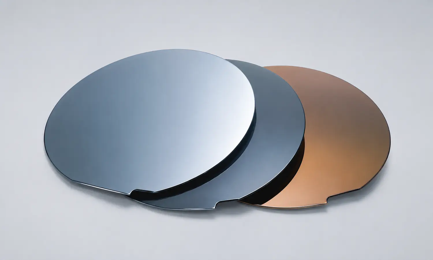
Specify wafer diameter and technical requirements together.
Complete the technical selections before adding the item. Unknown fields may remain blank; availability, lead time and commercial terms are confirmed in the quotation.
What do these options mean?
If you are unsure, choose the custom option in the RFQ. The technical team will clarify the required specification for the application.
SSP / DSP
Single-side or double-side polished wafer finish.
Orientation
The crystal plane, such as (100), (111) or an application-specific cut.
Off-axis
A controlled angular offset of the surface from the principal crystal plane.
Supply to technical specification; suitability and lead time are confirmed in the quotation.
State any required analysis certificate, drawing or test report. Available documents are confirmed for the product and delivery scope in the quotation.
Configure the requirement, not just the product name.
Built around the process.
Send the drawing, target value or process condition.
Our technical team will evaluate the feasible supply configuration before quotation.